Thick copper PCBs
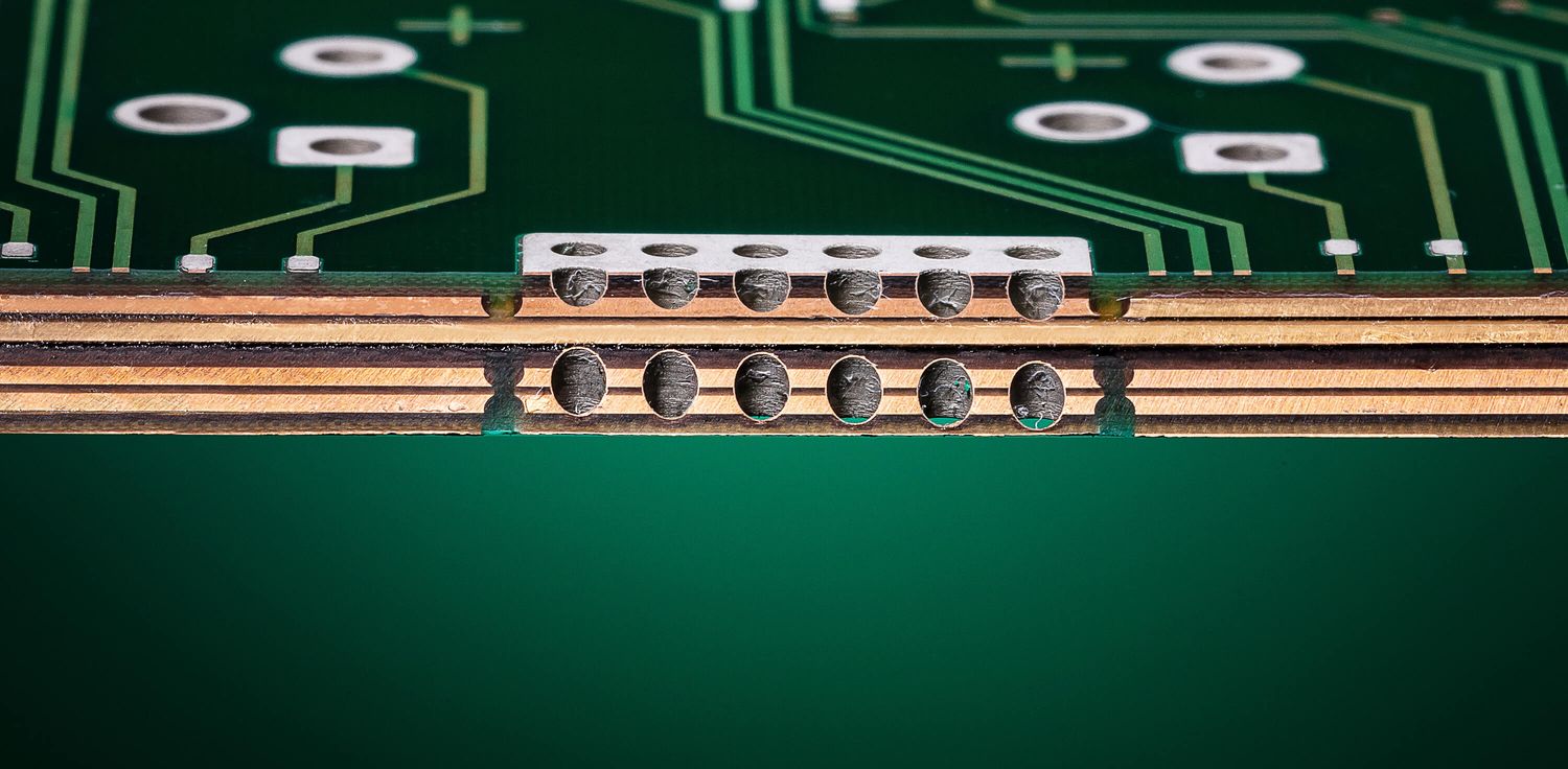
Thick copper PCBs, manufactured in genuine etching technology, are the first choice in case of high currents and characterised by structures with copper thicknesses from 105 to 400 µm.
- Home
- PCB Technologies
- Thick copper PCBs
Your advantages
- High currents and heat dissipation in the circuit board
- Targeted partial increase in cross-section for high-current paths
- Reduction of space requirements for high-current conductor systems
- From sample to series production from a single source
- Power and control electronics on a single board
- PCB production and processing with standard materials and series processes
- Cost optimisation of the final product
We are happy to support your thick copper project at every step along the way.
Contact our expert team here.
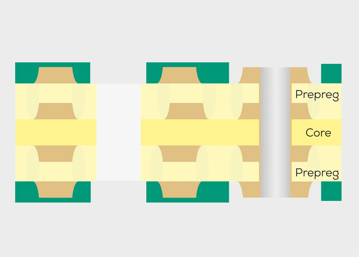
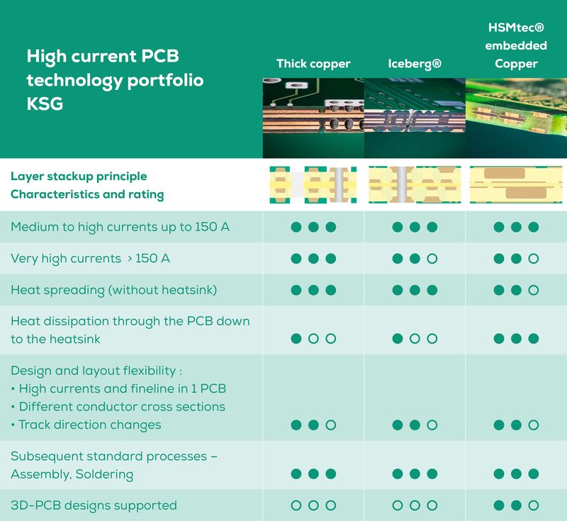
This PCB classic is the first choice when high currents are unavoidable: the thick copper PCB, manufactured in genuine etching technology. Thick copper PCBs are characterised by structures with copper thicknesses from 105 to 400 µm. These PCBs are used for large (high) current outputs and for optimisation of the thermal management. The thick copper allows large PCB-cross-sections for high current loads and encourages heat dissipation. The most common designs are multilayer or double-sided. With this PCB technology it is also possible to combine fine layout structures on the outer layers and thick copper layers in the inner layers.
| Materials | FR4 (thermostable) |
| Number of layers | 2-8 |
| PCB thickness | 0.5 mm - 3.2 mm |
| Final copper outer layers | 50, 70, 105, 175, 210 µm |
| Final copper inner layers | 70, 105, 210, 400 µm |
| Conductor structures | Depending on final copper according to design compass |
| Minimum drilling diameter | min. ⅔ of the total copper thickness |
| Aspect ratio | ≤ 1:6 |
| Surfaces | See general technical specifications, No HAL |
The values specified represent the maximum range of services and may be restricted in certain combinations.
- Chemical nickel/gold
- Chemical tin
- Electroplated nickel/gold
- OSP
- others on request
Solder resist masks
- Photosensitive coating systems, thermal final curing
- Colours: green, red, blue, glossy black, matt black, white, yellow
- Non-photosensitive coating systems, purely thermosetting: white, black
Additional printing
- Identification/assembly
- Hole filler/through hole filler
- Peelable solder mask
- Heatsink
- Carbon
Edge plating
The end faces of the PCB contour can be plated in order to improve the EMC protection of a PCB, make electrical contact with the housing of the module or meet increased cleanliness requirements.
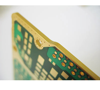
Milled plated through holes
It is possible to produce application-specific components with so-called milled plated through holes. Due to the possibility of contact on the front side, the resulting PCBs can be soldered as components to another board (interposer).
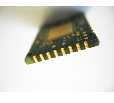
Contour machining
Contour production: milling and scoring
- Use filled thermostable base materials with low Z-axis expansion
- Calculate resin filling level (material-dependent pre-calculation using layer stack-up at KSG)
- Use sufficient resin-rich prepregs
- Avoid "stacked" copper surfaces and copper-free areas across all layers of the layer stack up
- Evenly distribute copper surfaces and copper-free areas
- Fill large copper-free areas with copper
- Generate sufficiently large residual rings
Calculate your high current tracks with our calculator
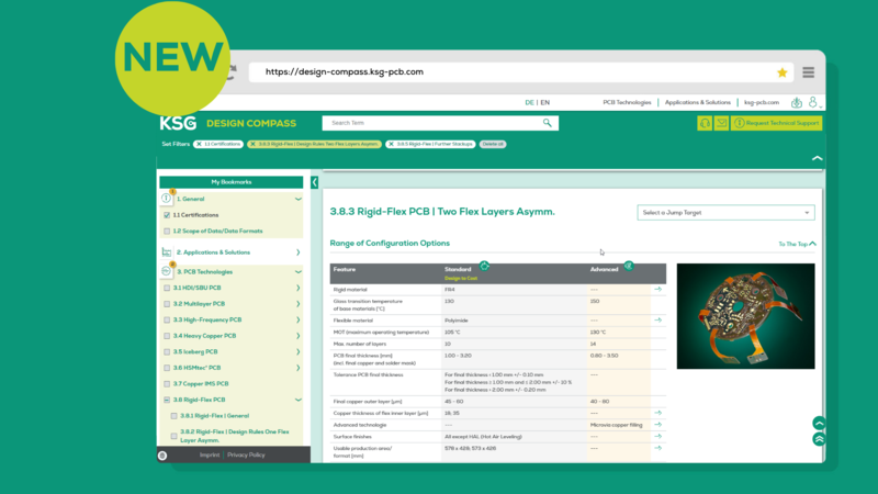
Digital Design Compass
The smart platform for fast and reliable PCB development.
- 2 plants. 1 platform. Available 24/7.
- Design rules for all technologies
- Practical examples and design-to-cost tips
We’ve combined all the parameters for you in our Design Compass.
A safe track to be smarter together
Take advantage of the direct line to the experienced PCB experts in our Technical Support. We are happy to support you in every phase of your project.
When extremely high currents are required
Power and control electronics on a single board
Targeted partial increase in cross-section for high-current paths
