
 and via connection (laservia) possible")
Your advantages
- Production of application-specific systems (System-in-Package, SiP)
- Maximum miniaturisation possible
- Replaces board-to-board solutions
- Housing replacement/protection against accidental contact
- Optimised thermal and power distribution
- Improved EMC protection
- Shorter signal paths
- Complicated reverse engineering/plagiarism protection
- Protected from extreme environmental influences
- Protected from vibration, impact and pressure effects
Lack of space on the outer layers? Why not use an additional assembly layer inside the PCB? With its embedding technologies, KSG offers you the right solution for the integration of active and passive electronic components - up to a minimum size of 01005 and a maximum component height of 2.5 mm.
| Number of layers | ≥ 3 |
| PCB thickness | ≥ 0.25mm for assembly layer |
| Materials | FR4, other base materials on request |
| Glass transition temperature | 150°C, 170/180°C |
| Special features of components | Components with cavities or electrolytic capacitors unsuitable; Suitability of the components must be tested; Components with copper terminals are required for laser connection; maximum height 2.50 mm |
| Special features PCB | no HAL Design rules on request |
The specified values represent the maximum performance spectrum and may be restricted in certain combinations.
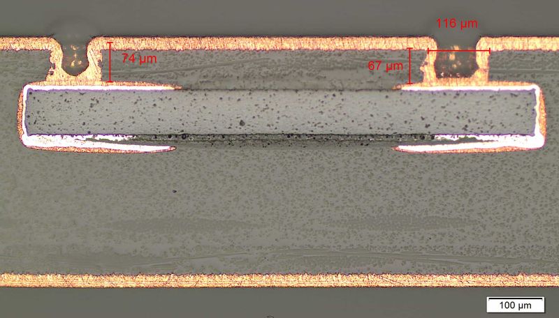
Cavity describes the production of one or more defined cavity in the PCB. The components are contacted electrically and mechanically using various methods.

The soldering process is used to place components on a PCB and embed them in the subsequent laminating multilayer in its composite. The electrical contact is made via the rewiring in the multilayer.

The components are bonded to a multilayer component, laminated into the composite and electrically connected by means of laser and subsequent electroplating. The components used have a terminal contact adapted to this technology.
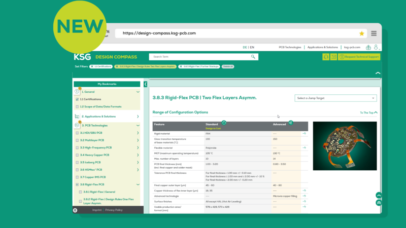
Digital Design Compass
The smart platform for fast and reliable PCB development.
- 2 plants. 1 platform. Available 24/7.
- Design rules for all technologies
- Practical examples and design-to-cost tips
We’ve combined all the parameters for you in our Design Compass.
A safe track to be smarter together
Take advantage of the direct line to the experienced PCB experts in our Technical Support. We are happy to support you in every phase of your project.


