

Your advantages
- High current paths carrying 400 amps and above
- Thermal management for power components (MOSFETs, IGBTs and others)
- Reduced system costs (logistics, procurement, manufacturing, quality assurance)
- Standard processes in production and further processing
- Increased efficiency and service life of components
- Increased reliability through the replacement of plug and cable connections, bus bars, etc.
- Reduced space, weight and volume for the application / PCB
- V-scoring enables three-dimensional self-supporting printed circuit board elements
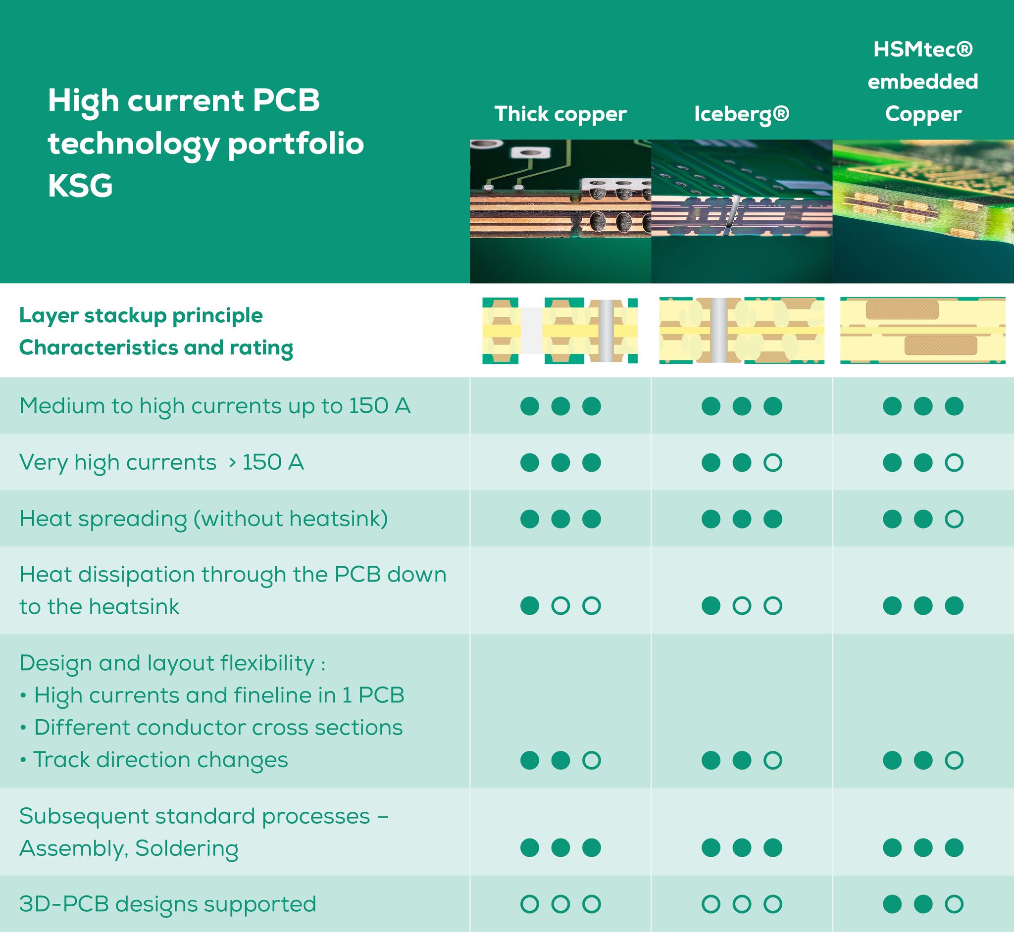
This PCB technology is highly suitable for applications where control and power electronics meet. In this case, there are often special challenges in the PCB layout, as different demands are made on the design. By partially integrating copper profiles into the printed circuit board, high current paths - or thermal management and fine conductor layout - can be easily combined and adapted to the spatial conditions. The diverse design variants allow high currents and heat losses from components to be directed specifically into PCBs - without any further external work steps.
This process for manufacturing printed circuit boards involves embedding copper profiles directly into the board and connecting them to the etched inner and/or outer layers by means of patented ultrasonic connection technology. This enables easy integration into a standard multilayer manufacturing process with subsequent pressing of the individual layers.
Copper elements with variable widths from 2 to 12 mm and individual lengths offer the greatest possible flexibility for the high-current layout and thermal design of the PCB. Performance can be significantly increased even with existing PCB designs.
| Materials | FR4 |
| Technology | High current, thermal management and 3D PCB |
| PCB thickness | 0.8 mm - 3.2 mm |
| Number of layers | 2 - 10 |
| Final copper | 35 - 105 µm |
| PCB layout | Depending on final copper according to design compass |
| Minimum drilling diameter | 0.25 mm; 0.50 mm through copper profiles |
| Aspect ratio | ≤ 1:8 |
| Solder resist masks | Photosensitive solder resist systems, UV solder mask systems Screen printing Colours: green, white, black matt |
| Surfaces |
|
| Bending angle | ≤ 90° |
The values specified represent the maximum performance spectrum and may be restricted may be restricted in certain combinations.
- Chemical nickel/gold
- Chemical tin
- Electroplated nickel/gold
- OSP
- others on request
Solder resist masks
- Photosensitive coating systems, thermal final curing
- Colours: green, red, blue, glossy black, matt black, white, yellow
- Non-photosensitive coating systems, purely thermosetting: white, black
Additional printing
- Identification/assembly
- Hole filler/through hole filler
- Peelable solder mask
- Heatsink
- Carbon
Edge plating
The end faces of the PCB contour can be plated in order to improve the EMC protection of a PCB, make electrical contact with the housing of the module or meet increased cleanliness requirements.

Milled plated through holes
It is possible to produce application-specific components with so-called milled plated through holes. Due to the possibility of contact on the front side, the resulting PCBs can be soldered as components to another board (interposer).

Contour machining
Contour production: milling and scoring
High currents directly integrated
High current and fine conductor structures on a printed circuit board are not contradictory - even within the same layer. Selective integration of large copper cross sections into the design of any layer of a standard multilayer board makes it possible to combine currents of up to 400 Ampere with even the finest conductor structures on a single printed circuit board.
This is achieved by embedding copper profiles directly into the PCB, and bonding them with the etched inner and outer layers using patented ultrasonic bonding technology.
- Currents up to 400 A
- Partial integration into FR4 multilayer PCBs
- Production and further processing in the standard process
- Customised solutions for every PCB design

Increase reliability. Reduce interfaces.
High-current connections integrated directly into the printed circuit board eliminate the need for separate circuit boards for control electronics. External components such as busbars, connection elements, plugs and cables are replaced, resulting in significantly increased reliability of the entire assembly.
- External components such as busbars, plugs, cables are no longer required.
- Increased reliability and quality
- Reduced space requirements & volumes
- Less interfaces/optimised EMC behaviour

The efficient dissipation of heat loss from modern power components ensures a longer service life of the module and optimises its efficiency. The partial integration of solid copper elements in FR4 PCBs enables the implementation of minimum thermal resistances for any component size and shape, which in turn enables the targeted avoidance of hotspots.
- Rapid heat dissipation of hotspots such as MOSFETs, IGBTs or LEDs through solid integrated copper
- Minimum thermal resistances due to direct contact by means of microvias
- Optional integrated insulation strength of more than 4 kV
- High current and thermal management on the same PCB
- Highly optimised service life / efficiency
Targeted reduction of system cost
The costs of installation, logistics, procurement and assembly are an increasingly critical factor in the design of an assembly. The complete integration of high current and control electronics into a single printed circuit board greatly reduces the total system cost compared to conventional PCB technologies.
- Reduction of system costs (logistics, procurement, installation, assembly, quality-assurance)
- External components such as busbars, plugs, cables are no longer required.

High performance in the minimum of space
HSMtec® PCBs provide the possibility to bend individual board parts once up to 90 degrees. Copper profiles integrated into the bending points provide mechanical stability and allow signal, high current and thermal connections between individual PCB segments to be implemented. Potential failure risks are thus minimised.
- Minimum space requirement due to integrated high current and thermal management
- 3D PCB designs for compact solutions

Our team provides uncomplicated, competent and active support in the implementation of your PCB application with the aim of meeting both technical and economic requirements.
- Creation of an individual concept based on your requirements
- Standard process implementation of the circuit board layout
- Support in the design, dimensioning and concept selection of your PCB
- Thermal measurements and analyses

Calculate your high current tracks with our calculator 
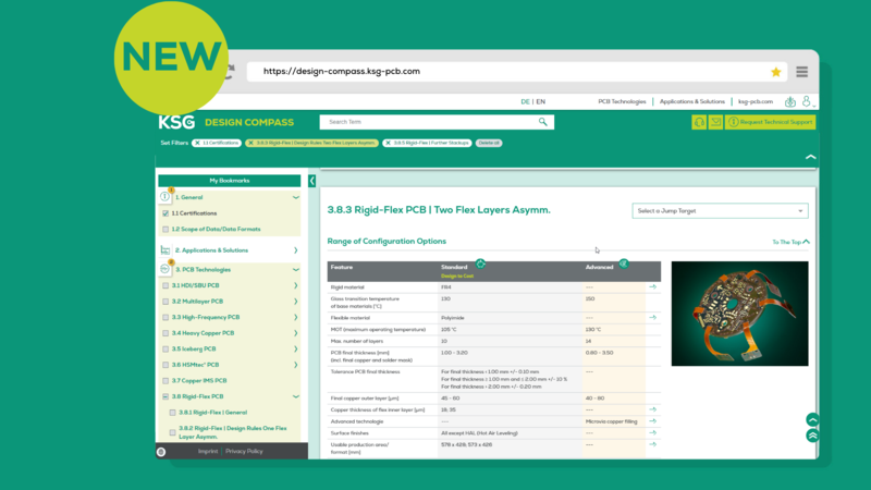
Digital Design Compass
The smart platform for fast and reliable PCB development.
- 2 plants. 1 platform. Available 24/7.
- Design rules for all technologies
- Practical examples and design-to-cost tips
We’ve combined all the parameters for you in our Design Compass.
A safe track to be smarter together
Take advantage of the direct line to the experienced PCB experts in our Technical Support. We are happy to support you in every phase of your project.


