Calculation of layer stack-ups
- Home
- Services
- Co-Engineering & Support
- Calculation of layer stack-ups
Doing calculations in advance always pays off.
Whether you’re trying to decide on the number of layers, the material or the minimum distances – choosing the right layer structure for your PCB opens up huge potential for optimisation with regard to producibility, service life and costs. And this is why it’s always worth carrying out calculations based on wide-ranging practical experience. In concrete terms: you tell us the thermal and electrical properties. We work out the optimal layer architecture, making sure that it’s technically feasible.
How exactly does this work? Using our proprietary KSG calculation tool. This tool allows us to combine real-life practical production findings with the knowledge of our PCB experts, allowing you to benefit from customised optimisations and a resource-efficient use of materials in your own specific layer structure. One thing always stays the same – for cost-optimised production, we recommend having a homogeneous and symmetrical copper layer and a symmetrical layer structure.

Here's what you can expect for your layer structure:
- Compliance with the required minimum distances between the individual layers
- Optimum resin filling of the conductor structures
- Dielectric spacing for impedance structures
- Compliance with the required total thickness
- Optimisation with regard to torsion and curvature
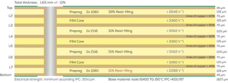
Example calculation of layer structure

The KSG support line
Use this direct line to get in touch with the experienced PCB experts on our technical support team.

