High frequencies. Reliable fault-free operation.
Higher transmission frequencies, shorter pulse rise times and quicker communication between components. And right at the centre – the PCB with its tracks acting as an important transmission line. High-frequency applications place increasingly high demands on the assembly, and require powerful and fault-free impedance behaviour. For the PCB specifically, if transmission errors are to be avoided, a number of influencing factors need to be taken into account across all stages of PCB development – from the layer structure to the layout right through to production.
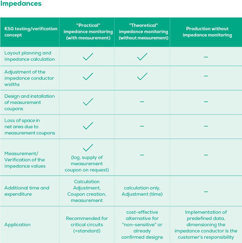
Thanks to our long-standing experience with high-frequency PCBs, we understand just how complex and sensitive impedance values can be, and we provide tailored support with both theoretical calculations and practical optimisations. With our state-of-the-art software, you can model your PCB structure and accurately simulate any changes to the track parameters. We use real process experience and production tolerances to predict the exact impedance characteristics of your PCB, and we work with you to optimise these characteristics if necessary.

The following software tools and measurement techniques are used at KSG:
- Compliance with the required minimum distances between the individual layers
- Optimum resin filling of the conductor structures
- Dielectric spacing for impedance structures
- Compliance with the required total thickness
- Optimisation with regard to torsion and curvature