Thermal analyses
- Home
- Services
- Co-Engineering & Support
- Thermal analyses
Reliable prevention of hotspots
Temperature differences are a major risk factor for the service life of an electronic component. It’s therefore important to work out how to optimally distribute the heat on the PCB in a way that ensures thermal equilibrium.
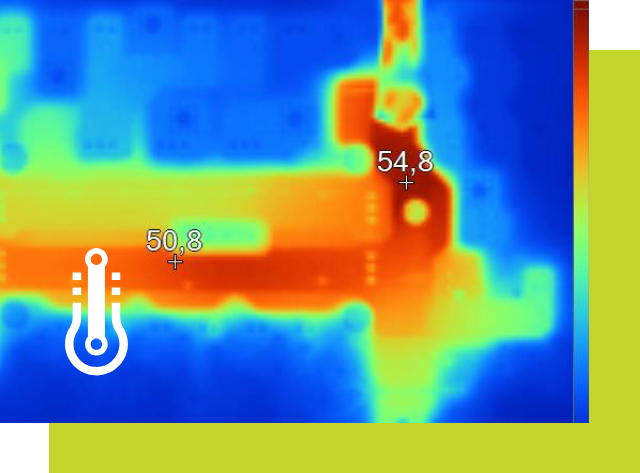
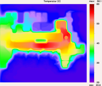
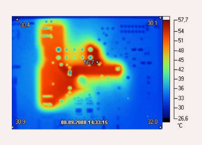
We offer a two-stage service for thermal analyses: we provide software-based, thermographic simulations during the development and layout creation stages, as well as real load tests following the production of the initial prototypes. Both of these processes have the same goal: to detect and eliminate any hotspots and risk factors in the layout prior to series production.

For the software-based, thermographic simulation, modelling is based on the layout data from Gerber data and other specifications, for example. Additional information such as layer structure, base material, system structure, component characteristics, current ratings, ambient conditions and installation situation are also important in order to represent actual conditions as accurately as possible. From that information, the software calculates the expected temperatures using the finite elements method and represents them as a thermographic image.

In the second stage, we test your PCB in the high-current laboratory under real conditions. Two high-current generators and a thermal imaging camera are used to apply actual currents to the high-current connections. After thermal equilibrium has been reached, the thermal imaging camera performs a surface measurement.

The KSG support line
Use this direct line to get in touch with the experienced PCB experts on our technical support team.

