

Your advantages
- Cost-effective 3D PCB technology
- Printed circuit board samples produced in series quality
- Increased reliability thanks to elimination of fragile connectors
- Miniaturisation of assemblies
- Reduction in processing steps for the further processing of assemblies
- Cost savings and minimisation of errors through the replacement of plug and soldered connections
- Optimised parts and logistics management
- Reduced assembly and testing effort
The semi-flex printed circuit board belongs to the 3D printed circuit board product group. This technology is suitable for double-sided and multilayer PCBs. The semiflexible design also offers significant cost advantages over classic rigid-flex PCBs and is ideally suited for static bending stress during assembly and installation.
In addition to the appealing price and the good static bending load during assembly and installation, semi-flex PCBs are characterized by the following parameters:
- Bending radius of at least 3 mm (semi-flex2 - rigid-flex technology) and at least 5 mm (semi-flex1 - deep-milled)
- Maximum bending angle of 180°
The manufacturing process for a semi-flex PCB is simple and based on the production process of a standard rigid FR4 PCB. A flexible cover layer is then applied over the desired bending area, instead of the standard solder mask ink. At the end of the manufacturing process the area below this flexible cover layer is deep-milled. This means that the thickness of the PCB in the bending area is reduced until the material can be easily bent.

| Materials | Polyimide / FR4 |
| Number of layers | 2-10 |
| PCB thickness | 0.6 – 3.2 mm |
| Final copper | 18, 35, 70 µm |
| Conductor structures | Depending on final copper according to design compass |
| Minimum drilling diameter | 0.20 mm |
| Solder masks | See general technical specifications |
| Surfaces | See general technical specifications |
| Contour production | Milling Scoring / breakaway tabs |
| Bending radii | ≥ 5 mm |
| Bending angle | ≤ 180° |
The values specified represent the maximum performance spectrum andmay be restricted in certain combinations.
- Chemical nickel/gold
- Chemical tin
- Electroplated nickel/gold
- OSP
- others on request
Solder resist masks
- Photosensitive solder mask systems
- UV solder mask system: Screen printing
- Colours: green, red, blue, glossy black, matt black, white, yellow,
- Flexlack: green
Additional printing
- Identification/assembly
- Hole filler/through hole filler
- Peelable solder mask
- Heatsink
- Carbon
Edge plating
The end faces of the PCB contour can be plated in order to improve the EMC protection of a PCB, make electrical contact with the housing of the module or meet increased cleanliness requirements.

Milled plated through holes
It is possible to produce application-specific components with so-called milled plated through holes. Due to the possibility of contact on the front side, the resulting PCBs can be soldered as components to another board (interposer).

Contour machining
Contour production: milling and scoring
Asymmetrical with a Cu layer in the flex area (deep-milled)
")
Asymmetrical with two Cu layers in the flex area (deep-milled)
")
Asymmetrical with one Cu layer in the flex area (SF technology)
")
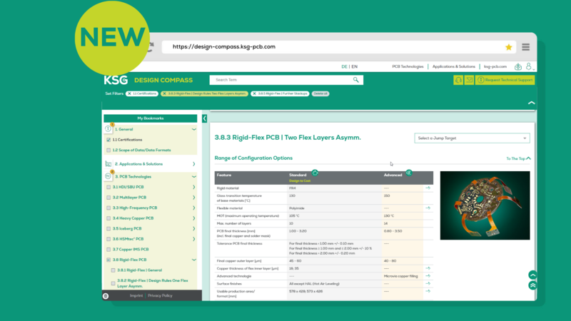
Digital Design Compass
The smart platform for fast and reliable PCB development.
- 2 plants. 1 platform. Available 24/7.
- Design rules for all technologies
- Practical examples and design-to-cost tips
We’ve combined all the parameters for you in our Design Compass.
A safe track to be smarter together
Take advantage of the direct line to the experienced PCB experts in our Technical Support. We are happy to support you in every phase of your project.


